| CPC H10K 59/131 (2023.02) | 20 Claims |
|
1. A display device comprising:
a substrate including a display area, a peripheral area surrounding the display area and including a first peripheral area and a second peripheral area, a first pad area disposed along a first side of the peripheral area, and a second pad area disposed along a second side of the peripheral area opposite the first side of the peripheral area;
a gate line disposed on the display area;
a first upper power line disposed on the first pad area;
a conductive member disposed on the first peripheral area, which is adjacent to the first pad area;
a protective insulating layer disposed on the conductive member;
a planarization layer disposed on the protective insulating layer;
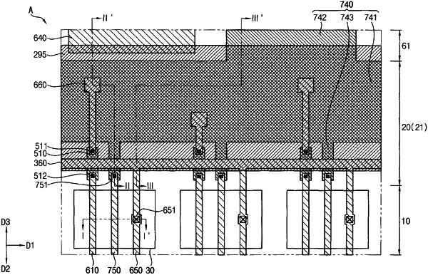
an upper connection member disposed on the planarization layer such that the upper connection member overlaps both the first pad area and the first peripheral area, the upper connection member electrically connecting the first upper power line and the conductive member to each other through a first contact hole, which is formed in both the protective insulating layer and the planarization layer and is disposed on a portion of the conductive member, and a second contact hole, which is formed in both the protective insulating layer and the planarization layer and is disposed on a portion of the first upper power line; and
a sub-pixel structure disposed on the protective insulating layer such that the sub-pixel structure overlaps the display area, wherein:
the sub-pixel structure comprises a thin film transistor, and
a gate electrode of the thin film transistor is electrically connected to the gate line.
|
|
3. A The display device comprising:
a substrate including a display area, a peripheral area surrounding the display area and including a first peripheral area and a second peripheral area, a first pad area disposed along a first side of the peripheral area, and a second pad area disposed along a second side of the peripheral area opposite the first side of the peripheral area;
a first upper power line disposed on the first pad area;
a conductive member disposed on the first peripheral area, which is adjacent to the first pad area;
a protective insulating layer disposed on the conductive member;
a planarization layer disposed on the protective insulating layer;
an upper connection member disposed on the planarization layer such that the upper connection member overlaps both the first pad area and the first peripheral area, the upper connection member electrically connecting the first upper power line and the conductive member to each other through a first contact hole, which is formed in both the protective insulating layer and the planarization layer and is disposed on a portion of the conductive member, and a second contact hole, which is formed in both the protective insulating layer and the planarization layer and is disposed on a portion of the first upper power line; and
a sub-pixel structure disposed on the protective insulating layer such that the sub-pixel structure overlaps the display area, wherein:
the conductive member includes:
a first extension part extending in a first direction that is parallel to a top surface of the substrate, the first extension part being disposed on the first peripheral area; and
a second extension part extending from a first side of the first extension part in a second direction, which is a direction extending from the first peripheral area to the display area, the second extension part being disposed on both a portion of the first peripheral area and the display area, and
the first contact hole is disposed on a portion of the first extension part.
|
|
15. A display device comprising:
a substrate including a display area, a peripheral area surrounding the display area and including a first peripheral area and a second peripheral area, a first pad area disposed along a first side of the peripheral area, and a second pad area disposed along a second side of the peripheral area opposite the first side of the peripheral area;
a first upper power line disposed on the first pad area;
a second upper power line disposed on both the first pad area and the first peripheral area, the second upper power line being configured to provide a different voltage level than the first upper power line;
a conductive member disposed on the first peripheral area, which is adjacent to the first pad area, the second upper power line being closer to the substrate than both the first upper power line and the conductive member;
a protective insulating layer disposed on the conductive member;
a planarization layer disposed on the protective insulating layer:
an upper connection member disposed on the planarization layer such that the upper connection member overlaps both the first pad area and the first peripheral area, the upper connection member electrically connecting the first upper power line and the conductive member through a first contact hole, which is formed in both the protective insulating layer and the planarization layer and is disposed on the conductive member, and a second contact hole, which is formed in both the protective insulating layer and the planarization layer and is disposed on the first upper power line; and
a sub-pixel structure disposed on the protective insulating layer such that the sub-pixel structure overlaps the display area.
|