| CPC H10K 59/131 (2023.02) [G09G 3/3233 (2013.01); H10K 59/123 (2023.02); G09G 2300/0426 (2013.01); G09G 2300/0452 (2013.01); G09G 2300/0842 (2013.01); G09G 2310/0202 (2013.01); H10K 59/352 (2023.02); H10K 59/353 (2023.02)] | 18 Claims |
|
1. A display panel, comprising:
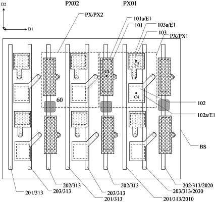
a plurality of pixel units, arranged on a base substrate in an array; each of the pixel units comprising a pixel circuit and a light-emitting element, the light-emitting element comprising a first electrode connected with the pixel circuit, and the plurality of pixel units comprising a plurality of first pixel units, a plurality of second pixel units, and a plurality of third pixel units, an effective light-emitting area of the first pixel unit being larger than an effective light-emitting area of the second pixel unit, and larger than an effective light-emitting area of the third pixel unit; and
a plurality of first data lines, each of the first data lines is configured to provide a first data signal to the pixel circuit of the first pixel unit,
wherein the first electrode of the first pixel unit, the first electrode of the second pixel unit, and the first electrode of the third pixel unit are arranged apart from each other, and an orthographic projection of the first data line on the base substrate is not overlapped with an orthographic projection of any one of the first electrode of the first pixel unit, the first electrode of the second pixel unit, and the first electrode of the third pixel unit on the base substrate;
the display panel further comprises a first insulating layer, and the first insulating layer comprises a first gate insulating layer, a second gate insulating layer, and an interlayer insulating layer which are stacked arranged;
the display panel further comprises a connection element, and a second insulating layer, wherein the first insulating layer, the connection element, and the second insulating layer are sequentially arranged from a position close to the base substrate to a position far away from the base substrate, the first electrode of the first pixel unit is connected with the pixel circuit through the connection element, the connection element is connected with the pixel circuit through a first via hole penetrating through the first insulating layer, and the first electrode is connected with the connection element through a second via hole penetrating through the second insulating layer, an orthographic projection of the first via hole on the base substrate is not overlapped with an orthographic projection of the second via hole on the base substrate; a distance between a second via hole of the third pixel unit and the first electrode of the first pixel unit which is closest to the second via hole of the third pixel unit is greater than or equal to 3.5 microns, and a distance between the second via hole of the third pixel unit and the first electrode of the second pixel unit which is closest to the second via hole of the third pixel unit is greater than or equal to 3.5 microns.
|