| CPC H10K 59/126 (2023.02) [G09G 3/3233 (2013.01); H10K 59/1213 (2023.02); G09G 3/3208 (2013.01); G09G 2300/0426 (2013.01); G09G 2300/0819 (2013.01); G09G 2300/0852 (2013.01); G09G 2310/0254 (2013.01); G09G 2320/0238 (2013.01); H01L 27/1222 (2013.01); H01L 27/1225 (2013.01); H01L 27/1251 (2013.01); H01L 29/04 (2013.01); H01L 29/78672 (2013.01); H01L 29/78675 (2013.01); H01L 29/7869 (2013.01); H10K 50/865 (2023.02); H10K 59/12 (2023.02); H10K 59/1216 (2023.02); H10K 59/131 (2023.02)] | 20 Claims |
|
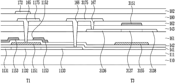
1. A display device comprising:
a light emitting diode electrically connected between a driving voltage line that transmits a driving voltage and a common voltage line that transmits a common voltage;
a driving transistor electrically connected between the driving voltage line and the light emitting diode;
a first transistor electrically connected between a first electrode of the driving transistor electrically connected to the driving voltage line and a data line that transmits a data voltage;
a second transistor electrically connected between a second electrode of the driving transistor electrically connected to the light emitting diode and a gate electrode of the driving transistor;
a third transistor electrically connected between the light emitting diode and an initialization voltage line that transmits an initialization voltage;
a fourth transistor electrically connected between the driving voltage line and the first electrode of the driving transistor; and
a sixth transistor electrically connected between the second electrode of the driving transistor and the light emitting diode, wherein
the driving transistor includes a polycrystalline semiconductor,
the second transistor and the third transistor each include an oxide semiconductor,
the third transistor includes a light blocking layer disposed directly on a same layer as the gate electrode of the driving transistor.
|