| CPC H10K 59/124 (2023.02) [H10K 71/00 (2023.02); H10K 77/111 (2023.02); H10K 59/1201 (2023.02); H10K 2102/311 (2023.02); H10K 2102/351 (2023.02)] | 16 Claims |

|
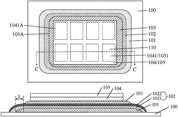
1. An Organic Light-Emitting Diode display substrate, comprising:
a first flexible organic layer;
a first inorganic layer on the first flexible organic layer;
a second flexible organic layer on the first inorganic layer;
a pixel driving circuit layer on the second flexible organic layer;
a light-emitting element layer on the pixel driving circuit layer;
wherein a thickness of the first flexible organic layer is 5 μm-20 μm, a thickness of the first inorganic layer is 0.4 μm-2 μm, and a thickness of the second flexible organic layer is 5 μm-20 μm;
wherein the first inorganic layer comprises a first inorganic sub-layer and a second inorganic sub-layer;
a material of the first inorganic sub-layer comprises one or more of silicon oxide, silicon nitride or silicon oxynitride,
wherein a thickness of the second inorganic sub-layer is 1 nm-50 nm.
|