| CPC H10K 59/1216 (2023.02) [H10K 59/1213 (2023.02); H10K 59/126 (2023.02); H10K 59/131 (2023.02); H10K 59/1201 (2023.02)] | 20 Claims |
|
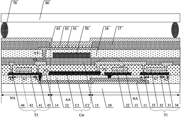
1. A display substrate, comprising: a base substrate and a plurality of sub-pixels disposed on the base substrate, wherein each sub-pixel comprises a light-emitting region and a non-light-emitting region, and a drive circuit is provided in each sub-pixel; the drive circuit comprises a storage capacitor and a plurality of transistors; the plurality of transistors comprise a switch transistor, a drive transistor and a sense transistor;
for each sub-pixel, the plurality of transistors are in the non-light-emitting region, the storage capacitor is a transparent capacitor, and an orthographic projection of the storage capacitor on the base substrate coincides with the light-emitting region; light emitted from the light-emitting region exits along a light exit direction, the light exit direction is a direction perpendicular to the base substrate and light exiting from a bottom of the base substrate, the storage capacitor is located at a side close to the base substrate along the light exit direction, and the light passes through the storage capacitor along the light exit direction and emits to the base substrate; a first electrode of the storage capacitor is disposed in a same layer as an active layer of the plurality of transistors and in a different layer from source and drain electrodes of the plurality of transistors, and a second electrode of the storage capacitor is on a side of the first electrode of the storage capacitor close to the base substrate; and
a first electrode of the drive transistor is connected to the second electrode of the storage capacitor through an active layer of the drive transistor, the active layer of the drive transistor is passed through a via of an insulating layer under the active layer of the drive transistor, extended to the second electrode of the storage capacitor and connected to the second electrode of the storage capacitor directly, a first electrode of the sense transistor is connected to the second electrode of the storage capacitor through an active layer of the sense transistor, and the active layer of the sense transistor is passed through a via of an insulating layer under the active layer of the sense transistor, extended to the second electrode of the storage capacitor and connected to the second electrode of the storage capacitor directly.
|