| CPC H10B 63/80 (2023.02) [G11C 7/12 (2013.01); G11C 13/0007 (2013.01); G11C 13/003 (2013.01); H10B 63/82 (2023.02); H10N 70/021 (2023.02); H10N 70/063 (2023.02); H10N 70/24 (2023.02); H10N 70/801 (2023.02); H10N 70/826 (2023.02); H10N 70/841 (2023.02); H10N 70/8833 (2023.02); G11C 2213/52 (2013.01); G11C 2213/77 (2013.01)] | 19 Claims |
|
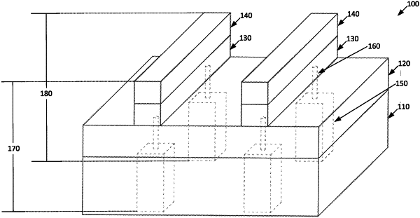
1. A resistive random access memory (RRAM) comprising:
one or more bottom electrodes comprised of tungsten;
one or more switching layers comprised of hafnium oxide disposed above the one or more bottom electrodes, the one or more switching layers comprising a switchable filament;
one or more resistive layers disposed above the one or more switching layers, wherein the one or more resistive layers are comprised of a conductive metal oxide; and
wherein each bottom electrode comprises a via disposed below the one or more switching layers, wherein the via is directly in contact with the switching layer and the via is comprised of tungsten.
|