| CPC H10B 63/30 (2023.02) [H10B 51/30 (2023.02); H10B 51/40 (2023.02); H10B 61/22 (2023.02); H10N 50/01 (2023.02); H10N 50/80 (2023.02); H10N 70/021 (2023.02); H10N 70/063 (2023.02); H10N 70/068 (2023.02); H10N 70/231 (2023.02); H10N 70/253 (2023.02); H10N 70/841 (2023.02)] | 20 Claims |
|
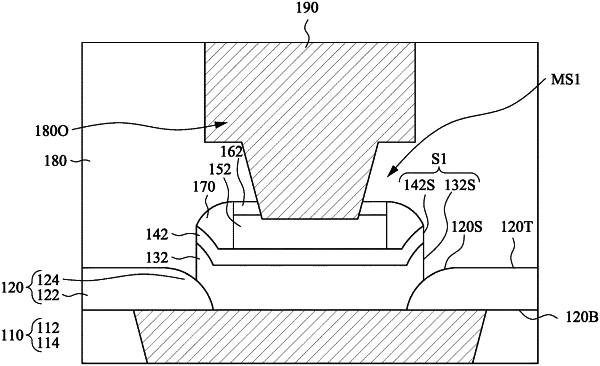
1. An integrated circuit, comprising:
a metal/dielectric layer having a first dielectric layer and a conductive feature in the first dielectric layer;
a second dielectric layer over the metal/dielectric layer;
a bottom electrode over the conductive feature and surrounded by the second dielectric layer, wherein the bottom electrode has a sidewall landing on a tapered sidewall of the second dielectric layer;
a resistance switch element over the bottom electrode; and
a top electrode over the resistance switch element.
|