| CPC H10B 61/00 (2023.02) [H10N 50/01 (2023.02)] | 20 Claims |
|
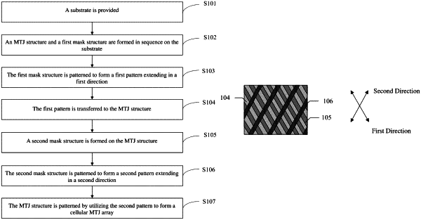
1. A method for manufacturing a semiconductor structure, comprising:
providing a substrate;
forming a magnetic tunnel junction (MTJ) structure and a first mask structure in sequence on the substrate;
performing a patterning process on the first mask structure to form a first pattern extending in a first direction;
transferring the first pattern to the MTJ structure;
forming a second mask structure on the MTJ structure;
performing a patterning process on the second mask structure to form a second pattern extending in a second direction, the first direction intersecting the second direction, and the first direction being not perpendicular to the second direction; and
performing a patterning process on the MTJ structure by utilizing the second pattern to form a cellular MTJ array, the first pattern and the second pattern together forming a cellular pattern.
|