| CPC H10B 51/20 (2023.02) [H01L 23/481 (2013.01); H10B 51/10 (2023.02)] | 20 Claims |
|
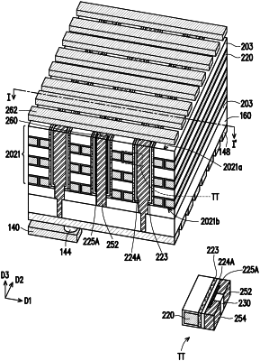
1. A memory device, comprising:
a first conductive via;
a first conductive line, disposed on and in physical contact with the first conductive via;
an etch stop layer, disposed on and in physical contact with the first conductive line;
a plurality of stacks, disposed on the etch stop layer; and
a first conductive pillar, wherein the first conductive pillar is an integrally formed element and extends from a first surface of the stacks to a surface of the first conductive line, and a second surface opposite to the first surface of the stacks is disposed between the first surface of the stacks and the surface of the first conductive line.
|