| CPC H10B 43/27 (2023.02) [H01L 21/02164 (2013.01); H01L 21/76802 (2013.01); H01L 21/76877 (2013.01); H01L 21/76895 (2013.01); H01L 23/5226 (2013.01); H01L 23/528 (2013.01); H01L 29/0847 (2013.01); H01L 29/1037 (2013.01); H10B 43/10 (2023.02); H10B 43/30 (2023.02); H10B 43/35 (2023.02); H10B 43/40 (2023.02); H10B 43/50 (2023.02); H01L 21/02271 (2013.01); H01L 21/0262 (2013.01); H01L 21/28568 (2013.01); H01L 21/31053 (2013.01); H01L 21/31111 (2013.01); H01L 21/31144 (2013.01); H01L 23/53214 (2013.01); H01L 23/53228 (2013.01); H01L 23/53257 (2013.01)] | 18 Claims |
|
1. A memory device, comprising:
a substrate;
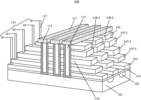
a stack comprising a first tier over the substrate and a second tier on the first tier, wherein each of the first tier and the second tier comprises gate material layers and insulating layers alternatingly arranged and extending along a first direction; and
a gate line slit extending along the first direction and dividing the stack into two portions,
wherein the stack comprises a connection portion that connects the two portions of the stack, the connection portion comprises at least two sub-connection portions along a second direction perpendicular to the first direction, the gate line slit comprises at least two portions along the first direction, and each sub-connection portion is between adjacent two portions of the gate line slit, a first sub-connection portion that connects the gate material layers of the first tier is different from a second sub-connection portion that connects the gate material layers of the second tier.
|