| CPC H10B 43/27 (2023.02) [H10B 41/10 (2023.02); H10B 41/27 (2023.02); H10B 41/35 (2023.02); H10B 43/10 (2023.02); H10B 43/35 (2023.02)] | 20 Claims |
|
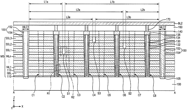
1. A nonvolatile memory device, comprising:
a mold structure that includes a plurality of word lines stacked on a substrate and first, second, and third string selection lines sequentially stacked on the plurality of word lines;
a plurality of channel structures that penetrates the mold structure and is connected to the substrate;
a first cutting region that cuts the mold structure;
a second cutting region that is spaced apart from the first cutting region in a first direction parallel to an upper surface of the substrate and that cuts the mold structure, the first and second cutting regions extending in a second direction intersecting the first direction, the first and second cutting regions being immediately adjacent to each other;
first, second and third cutting lines that extend in the second direction and cut at least one of the first, second and third string selection lines between the first cutting region and the second cutting region; and
a bit line on the mold structure extending in the first direction,
wherein the channel structures include first to fourth channel structures sequentially arranged in the first direction between the first cutting region and the second cutting region and electrically connected to the bit line.
|