| CPC H10B 43/27 (2023.02) [H10B 43/40 (2023.02)] | 14 Claims |
|
1. A method for forming a semiconductor device, comprising:
forming an insulating material layer over a substrate, wherein the substrate does not include single-crystalline silicon;
patterning the insulating material layer to form an isolation structure and a plurality of trenches in an upper portion of the isolation structure;
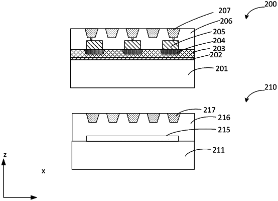
depositing a semiconductor material to fill up the plurality of trenches to form a plurality of array-base regions in the upper portion of the isolation structure, wherein the isolation structure is located between adjacent array-base regions and between the plurality of array-base regions and the substrate for electrically insulating the plurality of array-base regions from one another and from the substrate;
forming a plurality of memory arrays over the plurality of array-base regions;
forming an insulating structure to cover the plurality of memory arrays and the plurality of array-base regions;
forming a plurality of interconnect structures in the insulating structure;
bonding a peripheral structure including peripheral circuits to the insulating structure;
after the bonding, removing the substrate to expose the isolation structure; and
forming bonding pads on the isolation structure.
|