| CPC H10B 10/00 (2023.02) [H01L 21/563 (2013.01); H01L 23/5283 (2013.01); H01L 23/535 (2013.01); H01L 23/5386 (2013.01); H01L 24/09 (2013.01); H01L 24/32 (2013.01); H01L 25/0655 (2013.01); H01L 2224/02379 (2013.01); H01L 2224/32137 (2013.01)] | 20 Claims |
|
1. A chip package structure, comprising:
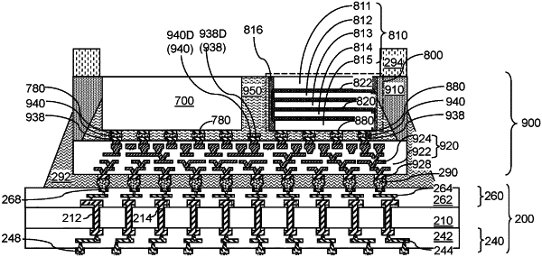
a fan-out package including a redistribution structure comprising redistribution-side bonding structures, a plurality of semiconductor dies comprising a respective set of die-side bonding structures that is attached to a respective subset of the redistribution-side bonding structures through a respective set of first solder material portions, a first underfill material portion which comprises a horizontally-extending portion that laterally surrounds the redistribution-side bonding structures and the die-side bonding structures of the plurality of semiconductor dies and contacts each of the first solder material portions,
wherein the plurality of semiconductor dies comprises a first semiconductor die having a first sidewall and a second semiconductor die having a second sidewall and disposed apart from the first semiconductor die in a plan view,
wherein a gap region laterally bounded by four vertical planes connecting two vertically-extending edges of the first sidewall and two vertically-extending edges of the second sidewall is present between the first sidewall and the second sidewall,
wherein the first underfill material portion further comprises a vertically-extending portion that is adjoined to the horizontally-extending portion, contacts the first sidewall and the second sidewall, fills an entirety of a volume of the gap region that is vertically bounded by a horizontal plane including top surfaces of the first semiconductor die and the second semiconductor die and by the horizontally-extending portion and laterally bounded by the four vertical planes,
wherein a subset of the redistribution-side bonding structures is electrically isolated from the plurality of semiconductor dies and the die-side bonding structures by the underfill material portion and is located entirely within an area of the vertically-extending portion of the underfill material portion in the plan view; and
a package substrate that is attached to the fan-out package via an array of second solder material portions.
|