| CPC H05K 3/244 (2013.01) [C25D 3/48 (2013.01); C25D 5/022 (2013.01); C25D 5/48 (2013.01); C25D 7/123 (2013.01); H05K 1/0296 (2013.01); H05K 1/09 (2013.01); H05K 1/11 (2013.01); H05K 3/108 (2013.01); H05K 3/181 (2013.01); H05K 3/188 (2013.01); C25D 3/38 (2013.01); H05K 2201/0338 (2013.01); H05K 2201/098 (2013.01); H05K 2201/0989 (2013.01); H05K 2201/099 (2013.01); H05K 2203/1184 (2013.01)] | 20 Claims |
|
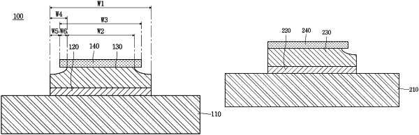
1. A circuit board comprising:
an insulating layer;
a first metal layer disposed on the insulating layer; and
a second metal layer disposed on the first metal layer such that the first metal layer is disposed between the second metal layer and the insulating layer,
wherein the first metal layer includes:
an upper surface in contact with the second metal layer;
a lower surface opposite from the upper surface and facing the insulating layer; and
a side surface disposed between the upper surface and the lower surface,
wherein at least a part of the side surface of the first metal layer overlaps the second metal layer in a vertical direction,
wherein the side surface of the first metal layer includes a curved portion,
wherein the first metal layer includes a first portion in which a width of the first metal layer gradually increases in the vertical direction from the upper surface of the first metal layer toward the lower surface of the first metal layer,
wherein the first portion of the first metal layer includes the curved portion of the side surface of the first metal layer, and
wherein the first metal layer includes:
a first region overlapped by the second metal layer in the vertical direction; and
a second region that is not overlapped by the second metal layer in the vertical direction.
|