| CPC H05K 1/116 (2013.01) [H05K 1/0298 (2013.01); H05K 3/4038 (2013.01); H05K 2201/09627 (2013.01)] | 20 Claims |
|
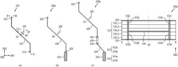
1. An electronic device comprising:
a multilayered base substrate including a plurality of substrate bases stacked on each other;
a first conductive via and a second conductive via penetrating the substrate bases and spaced from each other,
a conductive line electrically connecting the first conductive via and the second conductive via to each other and disposed on at least one of the substrate bases of the plurality of substrate bases, wherein the conductive line is disposed between an upper surface and a lower surface of the first conductive via; and
an open stub including a first end and a second end, wherein the first end is connected to a connector of the conductive line, and the second end is opened.
|