| CPC H05K 1/0306 (2013.01) [H05K 1/056 (2013.01); H05K 1/115 (2013.01)] | 17 Claims |
|
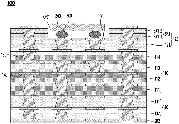
1. A circuit board comprising:
an insulating portion including a plurality of insulating layers;
a circuit pattern disposed on a surface of at least one insulating layer among the plurality of insulating layers; and
a via passing through at least one insulating layer among the plurality of insulating layers;
wherein the insulating portion includes:
a first insulating portion including at least one insulating layer, including a first insulating material; and
a second insulating portion disposed on the first insulating portion,
wherein the second insulating portion includes:
a first layer disposed on the first insulating portion and including a second insulating material different from the first insulating materials; and
a second layer disposed on the first layer and including a third insulating material different from the first and second insulating materials,
wherein the circuit pattern includes a first circuit pattern disposed on the second layer of the second insulating portion;
wherein the via includes a first via passing through the second layer of the second insulating portion and electrically connected to the first circuit pattern; and
wherein the second layer of the second insulating portion is a solder resist.
|