| CPC H03F 1/0288 (2013.01) [H03F 1/42 (2013.01); H03F 3/245 (2013.01); H03F 2200/451 (2013.01)] | 20 Claims |
|
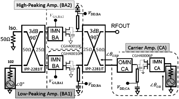
1. An asymmetrical load-modulated balanced amplifier, comprising:
a radio frequency (RF) input port;
a RF output port;
a peaking amplifier circuit operably coupled between the RF input and RF output ports, wherein the peaking amplifier circuit is a balanced amplifier that comprises a pair of asymmetrical power amplifiers, wherein each of the pair of asymmetrical power amplifiers of the peaking amplifier circuit has a different bias voltage, and wherein an asymmetry of the different bias voltages is swapped in dependence on a frequency of a signal received at the RF input port; and
a carrier amplifier circuit operably coupled to the RF input port.
|