| CPC H02H 9/02 (2013.01) | 18 Claims |
|
1. A current limiting circuit, comprising:
a first voltage terminal;
a second voltage terminal;
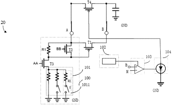
a first transistor, wherein an input terminal of the first transistor is electrically connected to the first voltage terminal, and an output terminal of the first transistor is electrically connected to the second voltage terminal; and
a current limiting module electrically connected to the input terminal of the first transistor and a control terminal of the first transistor,
wherein the current limiting module is configured to control voltage difference between the control terminal of the first transistor and the input terminal of the first transistor for controlling a state of the first transistor so that a current limiting value of the current limiting circuit is adjustable;
wherein the current limiting module comprises a second transistor, a first resistor, a third transistor, and a regulation unit,
wherein a first terminal of the second transistor is electrically connected to a first control terminal, a second terminal of the second transistor is electrically connected to the input terminal of the first transistor, and a third terminal of the second transistor is electrically connected to the control terminal of the first transistor,
wherein a first terminal of the first resistor is electrically connected to the input terminal of the first transistor, and a second terminal of the first resistor is electrically connected to the control terminal of the first transistor,
wherein a first terminal of the third transistor is electrically connected to a second control terminal, a second terminal of the third transistor is electrically connected to the control terminal of the first transistor, and a third terminal of the third transistor is connected to the regulation unit, and
wherein the regulation unit is configured to control the state of the first transistor.
|