| CPC H01Q 7/00 (2013.01) [H05K 3/341 (2013.01); H01Q 1/243 (2013.01)] | 17 Claims |
|
1. A circuit board assembly, comprising:
a connection circuit board including circuit board pads;
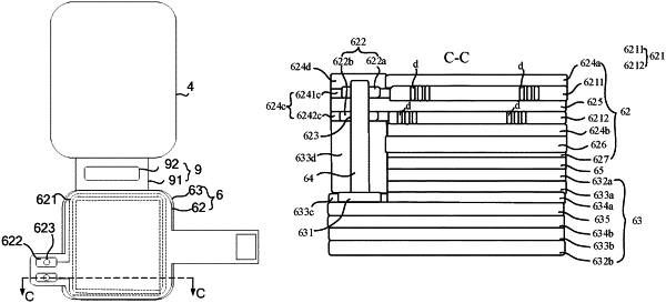
a near field communication antenna attached to the connection circuit board, wherein the near field communication antenna includes: an antenna coil, antenna pads electrically connected to the antenna coil, and through holes penetrating the antenna pads and disposed opposite to the circuit board pads; and
solders, wherein the solders are connected to the circuit board pads through the through holes, so that the antenna pads are electrically connected to the circuit board pads, respectively; wherein
the near field communication antenna further includes: a first insulating layer, a first coil, a first carrying layer, a second coil, a second insulating layer, a first adhesive layer and a magnetic material layer that are stacked in sequence; a first end of the first coil is electrically connected to a first end of the second coil to constitute the antenna coil;
numbers of the circuit board pads, the antenna pads, the through holes and the solders each are two;
the two antenna pads are both disposed on the first carrying layer, and are electrically connected to a second end of the first coil and a second end of the second coil in a one-to-one correspondence;
the two through holes are disposed opposite to the two circuit board pads in a one-to-one correspondence, and each through hole penetrates the first carrying layer and a corresponding antenna pad in the two antenna pads;
each solder is connected to a corresponding circuit board pad in the two circuit board pads through a through hole in the two through holes; and
the circuit board assembly further includes a second adhesive layer disposed between the magnetic material layer and the connection circuit board.
|