| CPC H01Q 1/52 (2013.01) [H01Q 1/38 (2013.01); H01Q 1/48 (2013.01); H04N 23/51 (2023.01); H04N 23/52 (2023.01); H04N 23/54 (2023.01)] | 20 Claims |
|
17. An electronic device comprising:
a rear plate disposed to cover a rear surface of the electronic device and including a recess structure provided in an edge area;
a camera bracket disposed along the recess structure and at least partially exposed outward;
a support bracket including a first side wall connected to the rear plate and a second side wall separated from the first side wall and connected to the camera bracket; and
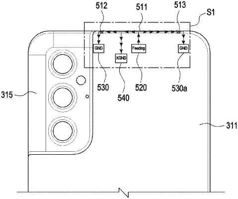
an antenna pattern formed on the support bracket and including a conductive portion forming at least a portion of the first side wall,
wherein at least one segmented portion located at one end of the conductive portion is spaced apart, by a first distance, toward the first side wall, from a first portion on the second side wall extending from the edge surface of the camera bracket,
wherein a ground portion connected to the conductive portion is located adjacent to the at least one segmented portion, and the ground portion is disposed between the camera bracket and the at least one segmented portion to electrically separate the conductive portion and the camera bracket,
wherein a feeding part is electrically connected to a printed circuit board (PCB) and the conductive portion, and
wherein the at least one segmented portion is located between the feeding part and the ground portion.
|