| CPC H01L 33/54 (2013.01) [H01L 25/0753 (2013.01); H01L 33/0075 (2013.01); H01L 33/10 (2013.01); H01L 33/24 (2013.01); H01L 33/32 (2013.01); H01L 33/36 (2013.01); H01L 33/385 (2013.01); H01L 33/44 (2013.01); H01L 33/46 (2013.01); H01L 33/50 (2013.01); H01L 33/505 (2013.01); H01L 33/52 (2013.01)] | 18 Claims |
|
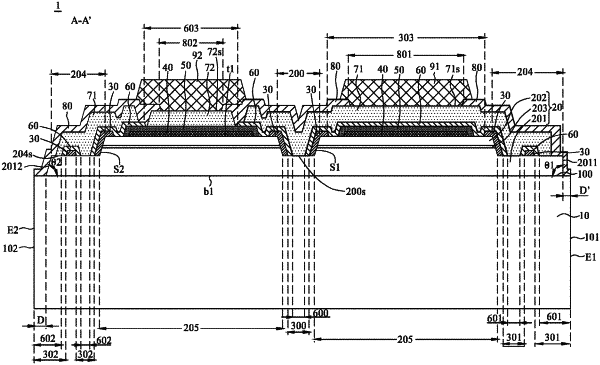
1. A light-emitting device, comprising:
a substrate including a top surface and a side surface;
a semiconductor mesa formed on the top surface of the substrate, including a first semiconductor layer, a second semiconductor layer, and an active layer formed between the first semiconductor layer and the second semiconductor layer;
a recess exposing the first semiconductor layer and surrounding the semiconductor mesa;
a first electrode pad formed on the semiconductor mesa and adjacent to a first edge of the light-emitting device; and
a second electrode pad formed on the semiconductor mesa and adjacent to a second edge of the light-emitting device,
wherein in a top view of the light-emitting device, the first edge and the second edge are formed on opposite sides of the light-emitting device, and the light-emitting device further comprises a third edge between the first edge and the second edge and connected to the first edge and the second edge, and
wherein the first semiconductor layer exposed by the recess and adjacent to the third edge comprises a first sidewall separated from the side surface of the substrate by a first space to expose the top surface of the substrate and a second sidewall separated from the side surface of the substrate by a second space to expose the top surface of the substrate, and the first space is smaller than the second space.
|