| CPC H01L 33/54 (2013.01) [H01L 33/005 (2013.01); H01L 33/10 (2013.01); H01L 2933/005 (2013.01)] | 20 Claims |
|
1. A method of manufacturing a substrate, comprising:
providing a substrate;
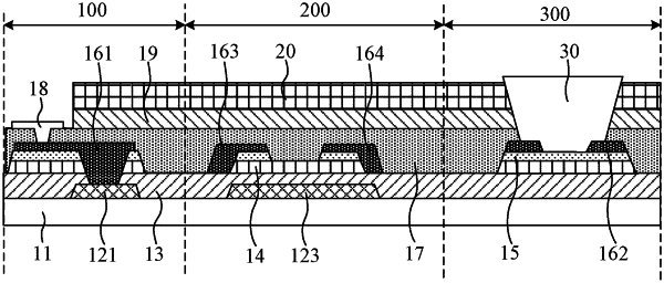
forming a light-emitting device binding terminal and a pixel driving circuit configured to drive a light-emitting device to emit light on one side of the substrate, wherein the light-emitting device binding terminal is disposed in a light-emitting device bonding area of the substrate, and the pixel driving circuit is disposed in a driving circuit area of the substrate;
forming a scratch-resistant layer on one side of the light-emitting device binding terminal away from the substrate, wherein the scratch-resistant layer covers the pixel driving circuit, and the scratch-resistant layer is patterned to form a first via hole, and the first via hole exposes the light-emitting device binding terminal;
filling solder paste into the first via hole by screen printing; and
stripping the scratch-resistant layer, wherein the light-emitting device is bound to the light-emitting device binding terminal by solder paste.
|