| CPC H01L 33/46 (2013.01) [H01L 27/156 (2013.01); H01L 33/10 (2013.01); H01L 33/382 (2013.01); H01L 33/62 (2013.01)] | 19 Claims |
|
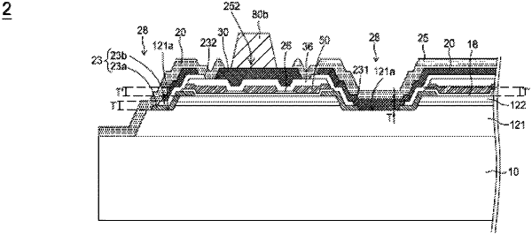
1. A light-emitting device, comprising:
a semiconductor stack comprising a first semiconductor layer, a second semiconductor layer and an active area between the first semiconductor layer and the second semiconductor layer, wherein the first semiconductor layer comprising an upper surface;
multiple exposed regions formed in the semiconductor stack to expose the upper surface, wherein in a top view, the multiple exposed regions are disposed in an inner region of the semiconductor stack;
a first reflective structure formed on the second semiconductor layer and comprising multiple openings and a periphery surrounding the multiple openings, wherein in the top view, a shortest gap between one of the multiple openings and one of the multiple exposed regions is d1, and a shortest gap between two adjacent openings of the multiple openings is d2, and d1 is greater than d2;
a second metal reflective structure formed on the first reflective structure, filled in the multiple openings, and electrically connected to the second semiconductor layer; and
a first protective layer covering the multiple exposed regions and a portion of the second semiconductor layer, and directly and physically contacting the semiconductor stack, wherein the first protective layer comprises an end portion contacting the upper surface and extending beyond a portion of the periphery of the first reflective structure in a cross-sectional view;
wherein the first reflective structure comprises dielectric material.
|