| CPC H01L 33/382 (2013.01) [H01L 33/10 (2013.01); H01L 33/20 (2013.01); H01L 33/32 (2013.01); H01L 33/62 (2013.01)] | 22 Claims |
|
1. A flip-chip light-emitting diode comprising:
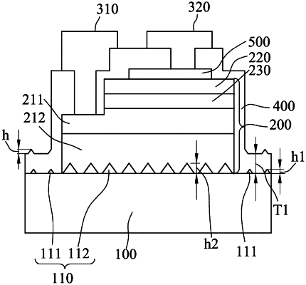
a substrate having a patterned surface formed with a protrusion unit, said patterned surface having a first patterned portion and a second patterned portion, said protrusion unit including a plurality of first protrusions formed on said first patterned portion and a plurality of second protrusions formed on said second patterned portion;
a light-emitting epitaxial layer disposed on said substrate, said light-emitting epitaxial layer including a first semiconductor layer, a second semiconductor layer and an active layer, said first semiconductor layer being disposed on said second patterned portion of said substrate to expose said first patterned portion, said active layer being interposed between said first semiconductor layer and said second semiconductor layer;
a first electrode connected to said first semiconductor layer;
a second electrode connected to said second semiconductor layer; and
a passivation layer having an epitaxial-covering portion disposed on said light-emitting epitaxial layer and a substrate-covering portion at least partially covering said first patterned portion of said substrate,
wherein said substrate-covering portion of said passivation layer has a top surface that is formed with hillocks, at least one of said hillocks having a height lower than that of at least one of said second protrusions formed on said second patterned portion of said substrate.
|