| CPC H01L 29/78696 (2013.01) [H01L 21/76224 (2013.01); H01L 29/66545 (2013.01); H01L 29/66742 (2013.01); H01L 29/78603 (2013.01)] | 20 Claims |
|
1. A method, comprising:
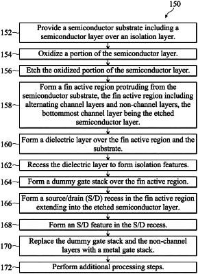
providing a substrate including a first semiconductor layer over a dielectric layer;
thinning the first semiconductor layer to a thickness less than a thickness of the dielectric layer;
forming a stack of alternating second semiconductor layers and third semiconductor layers over the thinned first semiconductor layer;
forming a fin active region protruding from the substrate, wherein the fin active region includes a portion of the thinned first semiconductor layer and the stack of alternating second semiconductor layers and third semiconductor layers disposed thereon, and wherein the forming of the fin active region exposes a portion of the dielectric layer;
forming isolation features over the exposed portion of the dielectric layer, wherein the isolation features cover sidewalls of the thinned first semiconductor layer;
forming a dummy gate stack over the fin active region;
forming a source/drain (S/D) recess in the fin active region adjacent to the dummy gate stack, wherein forming the S/D recess removes a portion of the thinned first semiconductor layer;
forming an epitaxial S/D feature in the S/D recess;
removing the second semiconductor layers to form openings between the third semiconductor layers, wherein the openings are formed adjacent to the epitaxial S/D feature; and
forming a metal gate stack in the openings and in place of the dummy gate stack.
|