| CPC H01L 29/7851 (2013.01) [H01L 21/324 (2013.01); H01L 21/823418 (2013.01); H01L 21/823431 (2013.01); H01L 29/0673 (2013.01); H01L 29/0847 (2013.01); H01L 29/41791 (2013.01); H01L 29/42392 (2013.01); H01L 29/513 (2013.01); H01L 29/66439 (2013.01); H01L 29/66795 (2013.01); H01L 29/775 (2013.01); H01L 29/78696 (2013.01); H01L 21/823412 (2013.01); H01L 21/823481 (2013.01)] | 20 Claims |
|
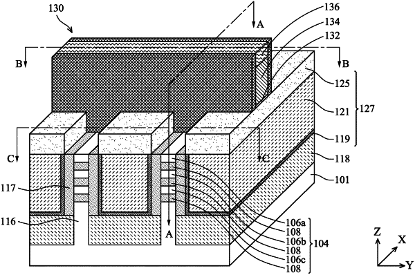
1. A transistor, comprising:
a first source/drain epitaxial feature;
a second source/drain epitaxial feature;
a first semiconductor layer disposed between the first and second source/drain epitaxial features, wherein the first semiconductor layer comprises a semiconductor material having a dopant at a first dopant concentration;
a second semiconductor layer disposed over the first semiconductor layer and between the first and second source/drain epitaxial features, wherein the second semiconductor layer comprises a semiconductor material having a dopant at a second dopant concentration;
a third semiconductor layer disposed over the second semiconductor layer and between the first and second source/drain epitaxial features, wherein the third semiconductor layer comprises a semiconductor material having a dopant at a third dopant concentration, wherein the first dopant concentration is substantially greater than the second dopant concentration, which is substantially greater than the third dopant concentration;
and
a gate electrode layer surrounding at least a portion of the first, second, and third semiconductor layers, wherein the transistor has two or more threshold voltages.
|