| CPC H01L 29/785 (2013.01) [H01L 29/42392 (2013.01); H01L 29/66545 (2013.01); H01L 29/6681 (2013.01); H01L 2029/7858 (2013.01)] | 20 Claims |
|
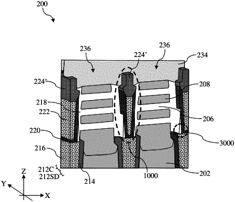
1. A semiconductor device, comprising:
a first source/drain feature and a second source/drain feature over a substrate;
a first plurality of nanostructures in contact with a sidewall of the first source/drain feature;
a second plurality of nanostructures in contact with a sidewall of the second source/drain feature;
a dielectric fin comprising:
a first portion sandwiched between the first source/drain feature and the second source/drain feature along a direction, and
a second portion disposed between the first plurality of nanostructures and the second plurality of nanostructures along the direction;
a gate structure wrapping around each of the first plurality of nanostructures and each of the second plurality of nanostructure as well as over the second portion; and
a contact etch stop layer (CESL) disposed over the first portion,
wherein sidewalls of the second portion of the dielectric fin taper toward the substrate, and
wherein the dielectric fin comprises:
an outer layer interfacing the first source/drain feature and the second source/drain feature,
an inner layer spaced apart from the first source/drain feature and the second source/drain feature by the outer layer, and
a helmet feature disposed on top surfaces of the outer layer and the inner layer.
|