| CPC H01L 29/78391 (2014.09) [H01L 29/401 (2013.01); H01L 29/516 (2013.01)] | 16 Claims |
|
1. An electronic device comprising:
a substrate;
a gate electrode on the substrate;
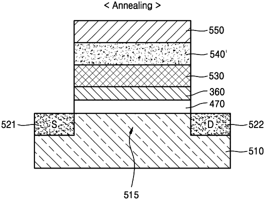
a ferroelectric crystallization layer between the gate electrode and the substrate, the ferroelectric crystallization layer being at least partially crystallized and including a dielectric material having ferroelectricity or anti-ferroelectricity;
a crystallization prevention layer between the ferroelectric crystallization layer and the substrate, the crystallization prevention layer including an amorphous dielectric material;
a high dielectric constant layer between the crystallization prevention layer and the substrate, the high dielectric constant layer including a different dielectric material than a material of the crystallization prevention layer; and
a high band gap layer between the high dielectric constant layer and the substrate, the high band gap layer including an amorphous dielectric material having a greater band gape than a material of the high dielectric constant layer.
|