| CPC H01L 29/7804 (2013.01) [H01L 29/7813 (2013.01); H01L 29/7831 (2013.01); H01L 29/0865 (2013.01)] | 4 Claims |
|
1. A semiconductor power device, comprising:
an n-type drain region, an n-type drift region located above the n-type drain region, at least one p-type body region located on a top of the n-type drift region, and a first n-type source region and a second n-type source region which are located within the at least one p-type body region, wherein a first current channel between the first n-type source region and the n-type drift region is formed in the at least one p-type body region;
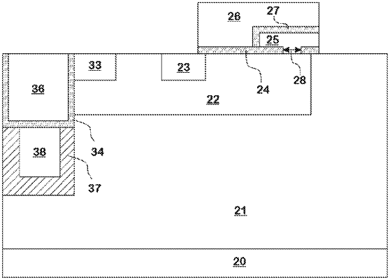
a first gate structure, which is configured to control a first current channel to be turned on or off, wherein the first gate structure comprises a first gate dielectric layer, a first gate and an n-type floating gate; the first gate and the n-type floating gate are located above the first gate dielectric layer; in a lateral direction, the n-type floating gate is located on a side close to the n-type drift region, the first gate is located on a side close to the first n-type source region and extends above the n-type floating gate, the first gate acts on the n-type floating gate through capacitive coupling; and the n-type floating gate contacts the p-type body region through an opening in the first gate dielectric layer to form a p-n junction diode in the opening, and the opening is located below the n-type floating gate, wherein the first gate extends above the n-type floating gate to cover two sidewalls of the n-type floating gate relative to the n-type drift region, and in the lateral direction, a distance from a center of the opening to a side end of the first gate dielectric layer close to the n-type drift region is less than a distance from the center of the opening to a side end of the first gate dielectric layer close to the first n-type source region; and
a second gate structure, which is configured to control a second current channel between the second n-type source region and the n-type drift region to be turned on or off, wherein the second gate structure comprises a gate trench recessed in the n-type drift region, and a second gate dielectric layer and a second gate which are located in the gate trench.
|