|
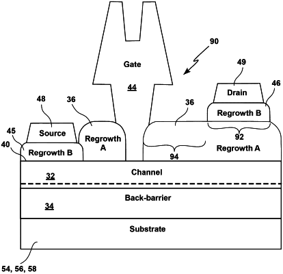
1. A HEMT comprising: a channel layer of a first III-Nitride semiconductor material, grown on a N-polar surface of a back barrier layer of a second III-Nitride semiconductor material; the second III-Nitride semiconductor material having a larger band gap than the first III-Nitride semiconductor material, such that a positively charged polarization interface and two-dimensional electron gas is obtained in the channel layer; a passivation, capping layer, of said first III-Nitride semiconductor material, formed on top of and in contact with a first portion of a N-polar surface of said channel layer; a gate trench traversing the passivation, capping layer, and ending at said N-polar surface of said channel layer; and a gate conductor filling said gate trench; a source contact layer of a fourth III-Nitride semiconductor formed on a second portion of said N-polar surface of said channel layer on a first side of said gate trench; and a drain contact layer of said fourth III-Nitride semiconductor, formed on a portion of a top surface of said passivation, capping layer, on a second side of said gate trench opposite said first side of said gate trench such that any portion of a bottom surface of said drain contact layer is separated from the channel layer by at least said passivation, capping layer.
|
