| CPC H01L 29/66553 (2013.01) [H01L 21/0217 (2013.01); H01L 21/02247 (2013.01); H01L 21/02252 (2013.01); H01L 21/02255 (2013.01); H01L 27/0886 (2013.01); H01L 29/0653 (2013.01); H01L 29/66545 (2013.01); H01L 29/6681 (2013.01); H01L 29/7853 (2013.01); H01L 21/30604 (2013.01); H01L 29/0673 (2013.01); H01L 29/42392 (2013.01)] | 20 Claims |
|
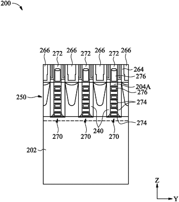
16. A device comprising:
a first semiconductor layer disposed on a substrate;
a second semiconductor layer disposed over the first semiconductor layer such that the second semiconductor layer is spaced apart from the first semiconductor layer;
an inner spacer extending from the first semiconductor layer to the second semiconductor layer, the inner spacer formed of remnants of at least one of the first and second semiconductor layers;
a source/drain feature interfacing with at least a portion of the inner spacer; and
a gate structure disposed on and wrapping around the first and second semiconductor layers, the gate structure including a gate dielectric layer having a first portion wrapping around the first and second semiconductor layers and a second portion disposed directly on a top surface of the inner spacer, the top surface of the inner spacer facing way from the substrate.
|