US 12,230,687 B2
Lateral gate material arrangements for quantum dot devices
Roza Kotlyar, Portland, OR (US); Stephanie A. Bojarski, Beaverton, OR (US); Hubert C. George, Portland, OR (US); Payam Amin, Portland, OR (US); Patrick H. Keys, Portland, OR (US); Ravi Pillarisetty, Portland, OR (US); Roman Caudillo, Portland, OR (US); Florian Luethi, Portland, OR (US); and James S. Clarke, Portland, OR (US)
Assigned to Intel Corporation
Filed by Intel Corporation, Santa Clara, CA (US)
Filed on Dec. 10, 2020, as Appl. No. 17/117,337.
Prior Publication US 2022/0190135 A1, Jun. 16, 2022
Int. Cl. H01L 29/49 (2006.01); B82Y 10/00 (2011.01); B82Y 30/00 (2011.01); G06N 10/00 (2022.01); H01L 29/06 (2006.01); H01L 29/15 (2006.01); H01L 29/423 (2006.01)
CPC H01L 29/4908 (2013.01) [G06N 10/00 (2019.01); H01L 29/0665 (2013.01); H01L 29/151 (2013.01); H01L 29/42392 (2013.01); B82Y 10/00 (2013.01); B82Y 30/00 (2013.01)] 21 Claims
OG exemplary drawing
 
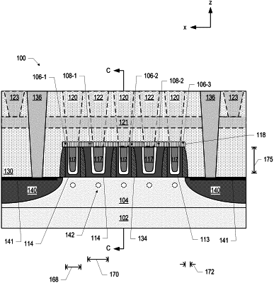
1. A quantum dot device, comprising:
a quantum well stack; and
a gate above the quantum well stack, wherein the gate includes a gate electrode, the gate electrode includes a first material proximate to side faces of the gate and a second material proximate to a center of the gate, one of the first material and the second material includes a p-type material, and another one of the first material and the second material includes an n-type material.