| CPC H01L 29/41791 (2013.01) [H01L 29/7851 (2013.01)] | 20 Claims |
|
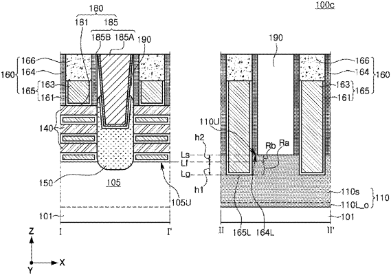
1. A semiconductor device comprising:
a plurality of active fins extending in a first direction on a substrate;
an isolation insulating layer provided between adjacent active fins of the plurality of active fins on the substrate and covering at least a portion of side surfaces of the plurality of active fins;
a plurality of channel layers stacked vertically and spaced apart from each other on the plurality of active fins;
a gate pattern extending in a second direction across the plurality of active fins and the plurality of channel layers on the substrate, the gate pattern surrounding at least a portion of each of the plurality of channel layers;
a plurality of spacer layers extending in the second direction across the plurality of active fins on both sides of the gate pattern; and
a plurality of source/drain regions provided on the plurality of active fins on both sides of the gate pattern, each of the plurality of source/drain regions being connected to a respective one of the plurality of channel layers,
wherein at least one of the plurality of spacer layers extends downwardly along a side surface of the gate pattern such that a lower surface of the at least one of the plurality of spacer layers is in contact with an upper surface of the isolation insulating layer, and the lower surface of the at least one of the plurality of spacer layers is at a level higher than a level of upper surfaces of the plurality of active fins, and
wherein the gate pattern has a lower surface contacting the isolation insulating layer, and the lower surface of the gate pattern is at a level lower than the level of the upper surfaces of the plurality of active fins.
|