| CPC H01L 29/0634 (2013.01) [H01L 29/1095 (2013.01); H01L 29/7802 (2013.01)] | 15 Claims |
|
1. A super junction MOSFET device, comprising:
a substrate having a first conductive type;
a buffer layer having the first conductive type and disposed on the substrate;
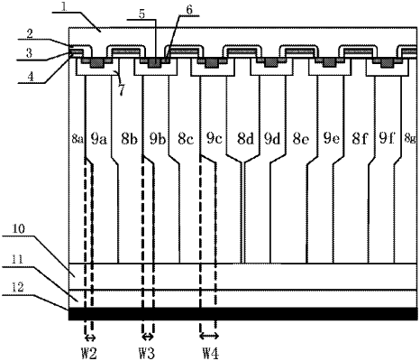
a super junction structure disposed on the buffer layer,
wherein the super junction structure comprises a plurality of first conductive type pillars and a plurality of second conductive type pillars alternately arranged in a transverse direction,
wherein each of the plurality of first conductive type pillars is adjacent to one of the plurality of second conductive type pillars, wherein a second conductive type is different from the first conductive type;
wherein lower portions of a first subset of the plurality of second conductive type pillars are shifted in a first direction for a first width, and lower portions of a second subset of the plurality of second conductive type pillars are shifted in the first direction for a second width; wherein the first width is different from the second width;
a body region having the second conductive type and disposed on a top of one of the plurality of second conductive type pillars;
a source structure located within the body region, wherein the source structure comprises a source region having the first conductive type and an ohmic contact region having the second conductive type, wherein the ohmic contact region is in contact with the source region; and
a gate structure in contact with one of the plurality of first conductive type pillars and the source structure.
|