| CPC H01L 28/92 (2013.01) | 16 Claims |
|
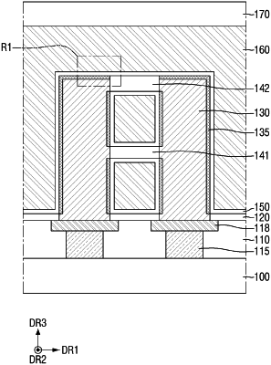
1. A semiconductor device comprising:
a landing pad on a substrate;
a lower electrode on the landing pad and electrically connected to the landing pad;
a capacitor dielectric film that is on the lower electrode and includes both a tetragonal crystal system and an orthorhombic crystal system;
a first doping layer that is between the lower electrode and the capacitor dielectric film and includes a first metal, the first doping layer physically contacting the lower electrode;
an upper electrode on the capacitor dielectric film;
a supporter pattern that is on at least one side of the lower electrode, wherein side walls of the supporter pattern are in direct contact with side walls of the lower electrode and a part of the first doping layer, and wherein an uppermost surface of the supporter pattern is in direct contact with the capacitor dielectric film;
wherein the first doping layer includes the first metal in an amount of 2 at % to 10 at %; and
wherein an uppermost surface of the first doping layer and the uppermost surface of the supporter pattern are coplanar.
|