| CPC H01L 28/55 (2013.01) [H01L 28/65 (2013.01); H01L 28/75 (2013.01); H01L 28/90 (2013.01); H01L 28/91 (2013.01); H10B 12/0335 (2023.02); H10B 12/315 (2023.02); H10B 12/34 (2023.02)] | 20 Claims |
|
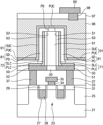
1. A semiconductor device comprising:
a substrate;
an insulating layer on the substrate;
a contact structure in the insulating layer;
a lower electrode on the contact structure, the lower electrode including a horizontal portion extending in a first direction that is parallel to a top surface of the substrate and a vertical portion extending in a second direction that is perpendicular to the top surface of the substrate;
a dielectric layer on the lower electrode; and
an upper electrode on the dielectric layer,
wherein the horizontal portion of the lower electrode includes first to fourth side surfaces,
the vertical portion of the lower electrode contacts the first side surface of the horizontal portion of the lower electrode, and
the dielectric layer contacts the second to fourth side surfaces of the horizontal portion of the lower electrode and covers a top surface of the vertical portion of the lower electrode.
|