| CPC H01L 27/156 (2013.01) [H01L 25/0753 (2013.01); H01L 27/153 (2013.01); H01L 33/08 (2013.01); H01L 33/30 (2013.01); H01L 33/405 (2013.01); H01L 33/62 (2013.01); G09G 3/32 (2013.01); G09G 2300/0404 (2013.01); G09G 2300/0426 (2013.01); G09G 2300/0452 (2013.01); H01L 33/22 (2013.01)] | 19 Claims |
|
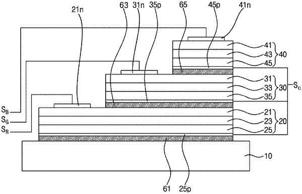
1. A light emitting apparatus, comprising:
a plurality of pixel regions disposed on a support substrate, each of the pixel regions including a plurality of subpixel stacks, each of the subpixel stacks including:
a first epitaxial stack disposed on the support substrate;
a second epitaxial stack disposed on the support substrate; and
a third epitaxial stack disposed on the support substrate,
wherein:
light generated from the first epitaxial stack is configured to be emitted outside and have a different peak wavelength from those emitted from the second and third epitaxial stacks;
light generated from the second epitaxial stack is configured to be emitted outside and have a different peak wavelength from that emitted from the third epitaxial stack;
during operation, one of the subpixel stacks within each pixel region is configured to be selected and driven;
each of the first, second, and third epitaxial stacks comprises a first conductivity type semiconductor layer, an active layer, and a second conductivity type conductivity type semiconductor layer; and
at least one subpixel stack further comprises an electrode disposed between the first epitaxial stack and the support substrate to be in ohmic contact with the first epitaxial stack.
|