| CPC H01L 27/156 (2013.01) [H01L 33/005 (2013.01); H01L 33/62 (2013.01); H01L 2933/0066 (2013.01)] | 18 Claims |
|
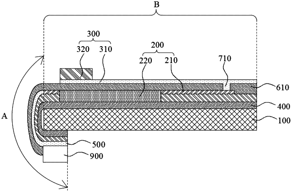
1. An array substrate, comprising a bonding region and a non-bonding region, wherein the array substrate further comprises:
a rigid substrate, in the non-bonding region;
a driving circuit layer, on a side of the rigid substrate and in the non-bonding region;
a light-emitting diode layer, on a side of the driving circuit layer away from the rigid substrate and being electrically connected to the driving circuit layer;
a flexible base layer, in the bonding region and on the same side of the rigid substrate as the driving circuit layer; and
a bonding wire layer, on a side of the flexible base layer away from the rigid substrate and being electrically connected to the driving circuit layer,
wherein the bonding wire layer and the flexible base layer is capable of being bent along an edge of the rigid substrate to a side of the rigid substrate away from the driving circuit layer;
wherein the flexible base layer extends to the non-bonding region and is between the rigid substrate and the driving circuit layer, or the flexible base layer extends to the non-bonding region and is between the driving circuit layer and the light-emitting diode layer.
|