| CPC H01L 27/14614 (2013.01) [H01L 27/14632 (2013.01); H01L 27/14643 (2013.01)] | 5 Claims |
|
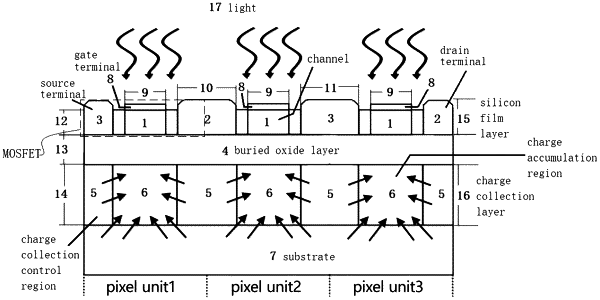
1. A UTBB photodetector pixel unit, comprising: a silicon film layer, a buried oxide layer, a charge collection layer and a substrate, the silicon film layer, the buried oxide layer, the charge collection layer and the substrate being arranged in sequence from top to bottom;
wherein the silicon film layer comprises NMOS transistors or PMOS transistors;
the charge collection layer is configured to form a centripetal electric field to collect photo-generated charges, and comprises charge collection control regions and charge accumulation regions; and
the substrate comprises: an N-type substrate or a P-type substrate;
wherein alternately arranged N-type wells and P-type wells are formed in the charge collection layer to serve as the charge collection control regions and the charge accumulation regions, respectively; wherein horizontal PN junctions between the P-type wells and the N-type wells are formed, and vertical PN junctions between the P-type wells and the N-type substrate are formed; and wherein the electric fields of the horizontal PN junctions and the vertical PN junctions together form the centripetal electric field; and
wherein in order to generate the centripetal electric field by the P-type wells, an N-type substrate is used and a voltage is applied to the N-type wells; if it is desired to generate the centripetal electric field by the N-type wells, a voltage is required to be applied to the P-type wells, and the substrate needs to use a P-type substrate.
|