| CPC H01L 27/1244 (2013.01) [H01L 27/1218 (2013.01)] | 12 Claims |
|
1. A stretchable pixel array substrate, comprising:
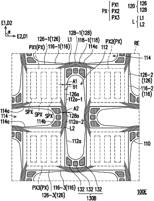
a base, having a plurality of first openings and a plurality of second openings, wherein each of the first openings has a first opening extending direction, and each of the second openings has a second opening extending direction, and the first opening extending direction and the second opening extending direction are different; the first openings and the second openings are alternately arranged in a first direction and a second direction to define a plurality of islands and a plurality of bridges of the base; the first direction and the second direction are interlaced, the first direction and the first opening extending direction are interlaced, and the second direction and the second opening extending direction are interlaced; each of the first openings has a plurality of opposite first edges and a plurality of opposite second edges, the first edges are arranged in the first direction and the second edges are arranged in the first opening extending direction; and each of the second openings has a plurality of opposite third edges and a plurality of opposite fourth edges, the third edges are arranged in the second direction, and the fourth edges are arranged in the second opening extending direction; and
a component layer, disposed on the base and comprising:
a plurality of island portions, having a plurality of pixel structures and respectively disposed on the islands of the base, wherein each of the plurality of pixel structures includes a first transistor and a pixel electrode, the first transistor has a first terminal, a second terminal, a control terminal and a semiconductor pattern, the first terminal and the second terminal are respectively electrically connected to two different regions of the semiconductor pattern, the pixel electrode is electrically connected to the second terminal of the first transistor, and a first insulating layer is sandwiched between the control terminal and the semiconductor pattern of the first transistor; and
a plurality of bridge portions, having a plurality of conductive wires and respectively disposed on the bridges of the base, wherein the conductive wires are electrically connected to the pixel structures;
the islands of the base comprise a first island and a second island arranged in the first direction;
the bridges of the base comprise a first bridge connecting the first island and the second island;
the island portions of the component layer comprise a first island portion and a second island portion respectively disposed on the first island and the second island of the base, and respectively having a first pixel structure and a second pixel structure of the pixel structures;
the bridge portions of the component layer comprise a first bridge portion disposed on the first bridge of the base and connecting the first island portion and the second island portion of the component layer; and the first bridge portion of the component layer has a first conductive wire of the conductive wires, and the first conductive wire electrically connects the first pixel structure and the second pixel structure;
a first edge of a first opening of the base has a first segment defining the first island of the base;
the first island portion of the component layer has an edge adjacent to the first opening, wherein the edge of the first island portion of the component layer refers to an edge of the first insulating layer; and
the first segment of the first edge of the first opening of the base and the edge of the first island portion of the component layer have a first distance in the first direction, and the first distance gradually increases closer to the first bridge of the base.
|