| CPC H01L 27/1225 (2013.01) [H01L 27/124 (2013.01); H01L 27/127 (2013.01)] | 4 Claims |
|
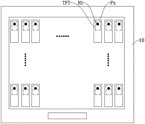
1. An array substrate, comprising a substrate and a plurality of sub-pixels distributed in an array on the substrate, wherein the sub-pixels comprise M oxide thin film transistors, and each of the oxide thin film transistors comprises a modulation electrode, a gate electrode, a source electrode, and a drain electrode which are arranged in a stack, wherein
the modulation electrodes of the M oxide thin film transistors are electrically connected to each other as a modulation layer, and the modulation layer is electrically connected to the gate electrode through N first vias, wherein M and N are both integers, and N<M;
the array substrate further comprising a first voltage-regulated signal line extending in a row direction, wherein the first vias of the plurality of the sub-pixels arranged in the row direction are aligned in the row direction and electrically connected to the first voltage-regulated signal line;
the array substrate further comprising a second voltage-regulated signal line extending in a column direction, wherein the first vias of the plurality of sub-pixels arranged in the column direction are aligned in the column direction and electrically connected to the second voltage-regulated signal line;
the array substrate further comprising the modulation layer, a buffer layer, a semiconductor layer, a gate-insulating layer, a gate electrode layer, a passivation layer, and a source and drain electrode layer which are successively formed on the substrate, wherein the modulation electrode is located in the modulation layer, the first voltage-regulated signal line and the second voltage-regulated signal line are located in the gate electrode layer, and the first vias penetrate the buffer layer and the gate-insulating layer.
|