| CPC H01L 27/0886 (2013.01) [H01L 21/823431 (2013.01); H01L 27/0207 (2013.01); H01L 29/0692 (2013.01); H01L 29/66545 (2013.01); H01L 27/0924 (2013.01); H01L 27/1211 (2013.01); H01L 29/7853 (2013.01); H01L 29/7855 (2013.01); H01L 29/7856 (2013.01); H10B 12/056 (2023.02); H10B 12/36 (2023.02)] | 20 Claims |
|
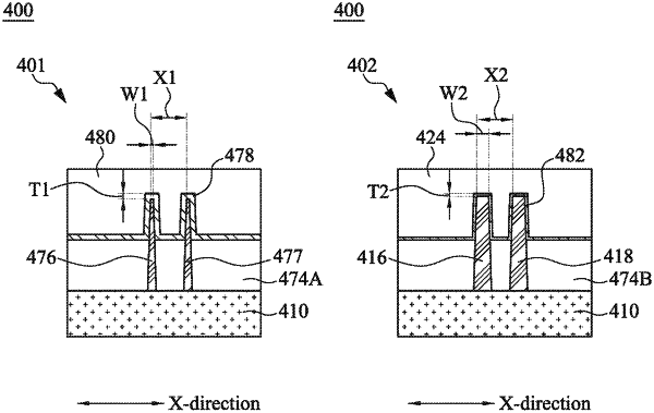
1. An integrated circuit (IC) structure, comprising:
a first circuit comprising a first semiconductor fin, a first gate electrode extending across the first semiconductor fin, and a first gate dielectric layer spacing the first gate electrode apart from the first semiconductor fin;
a second circuit comprising a second semiconductor fin, a second gate electrode extending across the second semiconductor fin, and a second gate dielectric layer spacing the second gate electrode apart from the second semiconductor fin; and
a third circuit comprising a third semiconductor fin, a third gate electrode extending across the third semiconductor fin, and a third gate dielectric layer spacing the third gate electrode apart from the third semiconductor fin,
wherein the first gate dielectric layer has a thickness greater than a thickness of the second gate dielectric layer, and the third semiconductor fin has a width less than a width of the second semiconductor fin.
|