| CPC H01L 25/167 (2013.01) [H01L 21/568 (2013.01); H01L 23/3157 (2013.01); H01L 23/5386 (2013.01); H01L 24/48 (2013.01); H01L 2224/48157 (2013.01)] | 19 Claims |
|
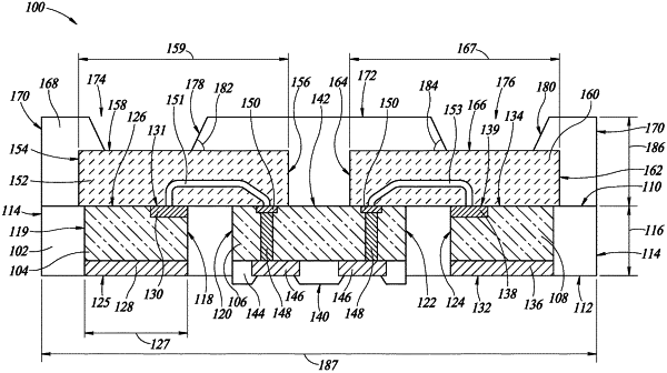
1. A device, comprising:
a first die having a first surface;
a second die having a second surface;
an interconnect substrate between and coupled to the first die and the second die, the interconnect substrate having a third surface;
a first resin covering respective sidewalls of the first die, the second die, and the interconnect substrate, the first resin spaces apart the first die, the second die, and the interconnect substrate from each other, the first resin includes a fourth surface substantially coplanar with the first, second, and third surfaces;
a first transparent portion on the fourth surface of the first resin, on the first surface of the first die, and on the third surface of the interconnect substrate; and
a second transparent portion on the fourth surface of the first resin, on the second surface of the second die, and on the third surface of the interconnect substrate, the second transparent portion spaced apart from the first transparent portion.
|
|
10. A device, comprising:
a first resin having a first surface and a second surface opposite to the first surface;
a first die in the first resin and extending from the first surface to the second surface;
a second die in the first resin and extending from the first surface to the second surface;
an interconnect substrate in the first resin and extending from the first surface to the second surface, the interconnect substrate coupled to the first die and the second die;
a first transparent portion on the first die and the interconnect substrate;
a second transparent portion on the second die and the interconnect substrate; and
a second resin on the first surface of the first resin and on the interconnect substrate, the second resin extending from the first transparent portion to the second transparent portion.
|
|
15. A device, comprising:
a first side and a second side opposite to the first side;
a first resin at the first side, the first resin including a first surface and a second surface opposite to the first surface;
a second resin on the first resin and at the second side, the second resin including a third surface coupled to the second surface, and a fourth surface opposite to the third surface;
a first die within the first resin, the first die extends from the first surface to the second surface;
a second die within the first resin, the second die extends from the first surface to the second surface;
a third die within the first resin, the third die extends from the first surface to the second surface, and the third die is between the first die and the second die;
a first transparent portion on the first die, on the third die, on the second surface of the first resin, and in the second resin;
a second transparent portion on the second die, on the third die, on the second surface of the first resin, and in the second resin;
a first opening in the second resin exposing a fifth surface of the first transparent portion;
a second opening in the second resin exposing a sixth surface of the second transparent portion;
a first electrical wire extends from the first die to the third die and extends through the first transparent portion, the first electrical wire electrically couples the first die to the third die; and
a second electrical wire extends from the second die to the third die and extends through the second transparent portion, the second electrical wire electrically couples the second die to the third die.
|