| CPC H01L 25/167 (2013.01) [H01L 24/83 (2013.01); H01L 24/95 (2013.01); H01L 27/1259 (2013.01); H01L 33/0093 (2020.05); H01L 24/24 (2013.01); H01L 24/29 (2013.01); H01L 24/32 (2013.01); H01L 24/73 (2013.01); H01L 33/20 (2013.01); H01L 33/32 (2013.01); H01L 2224/24051 (2013.01); H01L 2224/24105 (2013.01); H01L 2224/24147 (2013.01); H01L 2224/29006 (2013.01); H01L 2224/32013 (2013.01); H01L 2224/32058 (2013.01); H01L 2224/32148 (2013.01); H01L 2224/73204 (2013.01); H01L 2224/83201 (2013.01); H01L 2224/95101 (2013.01); H01L 2224/95133 (2013.01); H01L 2224/95136 (2013.01)] | 16 Claims |
|
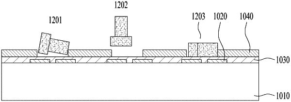
1. A method for manufacturing a display device, the method comprising:
forming an assembly electrode on a substrate;
applying an insulating layer on the assembly electrode;
disposing a partition wall on the insulating layer;
defining at least one assembly groove in the partition wall;
providing at least one light emitting diode (LED) having an assembly face corresponding to a shape of the at least one assembly groove in the partition wall; and
assembling the assembly face of the at least one LED into the at least one assembly groove in the partition wall,
wherein the at least one LED includes a first electrode, a first semiconductor layer, an active layer, a second semiconductor layer, and a second electrode stacked in a first direction to form a stacked structure,
wherein two opposing sides of the at least one LED are formed to have at least two longitudinal lengths, creating two flat assembly faces that correspond to a bottom surface of the at least one assembly groove, and
wherein the at least one LED is seated in the at least one assembly groove using one of the two flat assembly faces formed on the two opposing sides, and the at least one assembly groove is configured to accommodate a single LED.
|