| CPC H01L 25/105 (2013.01) [H01L 25/50 (2013.01); H01L 24/06 (2013.01); H01L 24/29 (2013.01); H01L 24/30 (2013.01); H01L 25/0657 (2013.01); H01L 2224/06181 (2013.01); H01L 2224/2919 (2013.01); H01L 2224/30181 (2013.01); H01L 2225/06541 (2013.01)] | 11 Claims |
|
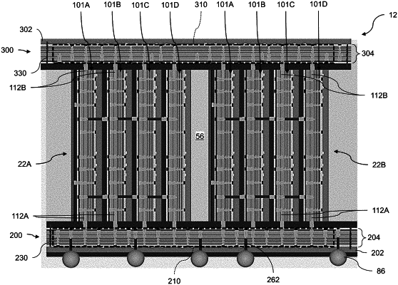
1. A method of manufacturing a semiconductor package, comprising:
bonding first dies to one another to form a first die stack having a first side and an opposing second side, each of the first dies comprising:
a planar first semiconductor substrate having a front side and an opposing back side that defines a plane of the first die; and
a first interconnect structure disposed on the front side of the first semiconductor substrate and comprising a first connection line and a second connection line;
planarizing the first side of the first die stack to expose the first connection lines; and
bonding the first side of the first die stack to a first connection die, such that the first connection lines are electrically connected to the first connection die, the first connection die comprising:
a planar first connection substrate having a front surface and an opposing back surface that defines a plane of the first connection die; and
a first connection interconnect structure disposed on the front surface of the first connection substrate and electrically connected to the first connection lines;
planarizing the second side of the first die stack to expose the second connection lines; and
bonding a second connection die to the second side of the first die stack, such that the second connection lines are electrically connected to a second connection interconnect structure of the second connection die,
wherein an angle formed between the plane of each first die and the plane of the first connection die ranges from about 45° to about 90°.
|