| CPC H01L 25/0657 (2013.01) [H01L 21/4853 (2013.01); H01L 21/568 (2013.01); H01L 23/3121 (2013.01); H01L 23/367 (2013.01); H01L 23/5389 (2013.01); H01L 24/32 (2013.01); H01L 21/561 (2013.01); H01L 2224/32055 (2013.01); H01L 2225/0652 (2013.01)] | 20 Claims |
|
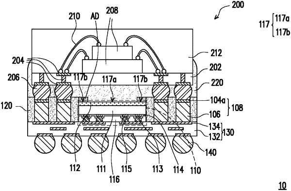
1. A semiconductor package, comprising:
a first semiconductor die;
an adhesive layer, directly adhered to peripheral regions of a top surface of the first semiconductor die;
a heat dissipation layer different from the adhesive layer, adhered to a central region of the top surface of the first semiconductor die and surrounded by the adhesive layer, wherein the heat dissipation layer is extended onto the entire central region between the peripheral regions of the top surface of the first semiconductor die;
a semiconductor device over the first semiconductor die; and
an underfill between the semiconductor device and the first semiconductor die, wherein the adhesive layer and the heat dissipation layer are in direct contact with the underfill.
|