| CPC H01L 25/0657 (2013.01) [G06F 1/3203 (2013.01); H01L 23/5384 (2013.01); H01L 23/5385 (2013.01); H01L 23/5386 (2013.01)] | 20 Claims |
|
1. A semiconductor device comprising:
a first semiconductor die that operates at a first power;
a second semiconductor die in a stack on the first semiconductor die that operates at a second power different than the first power; and
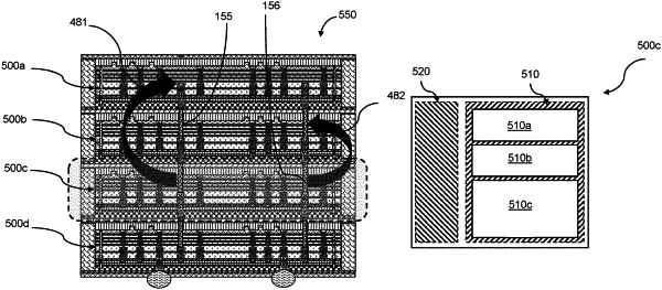
a power management semiconductor die in the stack that provides the first power to the first semiconductor die through a first via and provides the second power to the second semiconductor die through a second via, wherein the power management semiconductor die comprises:
a BCD area including a bipolar section, a CMOS section and a DMOS section; and
a core area including a plurality of processing elements adjacent the BCD area and having a size less than a size of the BCD area.
|