| CPC H01L 24/94 (2013.01) [H01L 21/768 (2013.01); H01L 21/7806 (2013.01)] | 20 Claims |
|
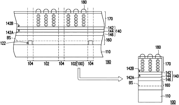
1. A method of fabricating a semiconductor chip, comprising:
form a first bonding layer on a first wafer substrate, the first bonding layer having a recess;
forming a circuitry structure and a second bonding layer on a second wafer substrate, the circuitry structure being located between the second wafer substrate and the second bonding layer;
bonding the second wafer substrate to the first wafer substrate by contacting the second bonding layer with the first bonding layer;
removing the second wafer substrate;
forming a conductor terminal on the circuitry structure, wherein the conductor terminal is positioned in a component region keeping from the recess of the first bonding layer; and
performing a singulation process to obtain a semiconductor chip comprising the circuitry structure and the conductor terminal, wherein the recess is separated from the semiconductor chip by the singulation process.
|