| CPC H01L 24/02 (2013.01) [H01L 21/56 (2013.01); H01L 23/3192 (2013.01); H01L 23/562 (2013.01); H01L 23/585 (2013.01); H01L 24/04 (2013.01); H01L 24/05 (2013.01); H01L 2224/02126 (2013.01); H01L 2224/0214 (2013.01); H01L 2224/02141 (2013.01); H01L 2224/02255 (2013.01); H01L 2224/02381 (2013.01); H01L 2224/0401 (2013.01); H01L 2224/05569 (2013.01)] | 20 Claims |
|
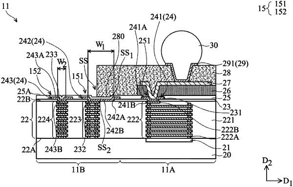
1. A package structure, comprising:
a substrate;
a first passivation layer formed over the substrate;
a metallization layer conformally formed on the first passivation layer, and a portion of the metallization layer extends into the first passivation layer;
a second passivation layer conformally formed on the first passivation layer and the metallization layer, wherein a step structure is formed on a top surface of the second passivation layer, and the step structure includes at least one lower part that is recessed from the top surface and lower than other parts of the step structure, wherein the at least one lower part is vertically aligned with the portion of the metallization layer; and
a polymer layer formed over the second passivation layer, wherein a portion of the polymer layer extends into the at least one lower part of the step structure to engage with the step structure.
|