| CPC H01L 23/576 (2013.01) [G01J 1/4257 (2013.01); G11C 29/12 (2013.01); H03K 19/00315 (2013.01)] | 18 Claims |
|
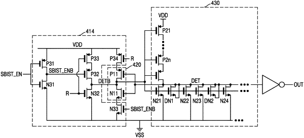
1. A laser detecting circuit comprising:
a latch circuit comprising a first inverter configured to invert a first output signal at a first node to generate a second output signal at a second node, and a second inverter configured to generate the first output signal based on the second output signal,
wherein the second inverter comprises a plurality of PMOS transistors connected in series between a first source voltage and the first node, and a plurality of NMOS transistors,
a gate of each of the plurality of PMOS transistors is connected to the second node, and a drain of each of the plurality of NMOS transistors is connected to the first node, and
the plurality of NMOS transistors comprises dummy NMOS transistors and normal NMOS transistors.
|